- English
-
EnglishDeutschItaliaFrançais한국의русскийSvenskaNederlandespañolPortuguêspolskiSuomiGaeilgeSlovenskáSlovenijaČeštinaMelayuMagyarországHrvatskaDanskromânescIndonesiaΕλλάδαБългарски езикGalegolietuviųMaoriRepublika e ShqipërisëالعربيةአማርኛAzərbaycanEesti VabariikEuskeraБеларусьLëtzebuergeschAyitiAfrikaansBosnaíslenskaCambodiaမြန်မာМонголулсМакедонскиmalaɡasʲພາສາລາວKurdîსაქართველოIsiXhosaفارسیisiZuluPilipinoසිංහලTürk diliTiếng ViệtहिंदीТоҷикӣاردوภาษาไทยO'zbekKongeriketবাংলা ভাষারChicheŵaSamoa日本語SesothoCрпскиKiswahiliУкраїнаनेपालीעִבְרִיתپښتوКыргыз тилиҚазақшаCatalàCorsaLatviešuHausaગુજરાતીಕನ್ನಡkannaḍaमराठी
Samsung Begins Development of 1nm Process Technology, Mass Production Targeted After 2029
According to industry sources on April 9, Samsung's Semiconductor Research Institute recently launched a development project focused on the 1nm process. Selected researchers who have been involved in cutting-edge processes such as 2nm have been reassigned to form the core of the new project team. Currently, the most advanced process on Samsung’s public foundry roadmap is the 1.4nm node, which is scheduled for mass production in 2027.
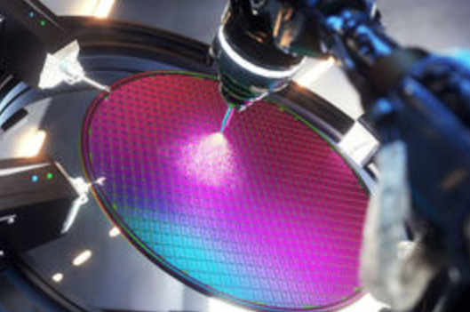
Achieving 1nm manufacturing will require an entirely new design paradigm, along with next-generation tools such as high numerical aperture extreme ultraviolet (High-NA EUV) lithography equipment. Reports suggest that Samsung is targeting a post-2029 timeline for mass production of this technology.
Samsung currently lags behind TSMC in 3nm process technology, which is already in production, and in the 2nm node expected to enter production this year. Notably, TSMC has reportedly achieved a yield rate of over 60% for its 2nm process—substantially ahead of Samsung—prompting the Korean tech giant to kick off development of the 1nm process earlier than initially planned.
At the same time, Samsung’s competitors are also moving forward with 1nm-class technologies. TSMC, for example, announced in April 2023 that it would begin production of its 1.6nm (16A) process—positioned between the 1.4nm and 2nm nodes—in the second half of 2026. This move is seen as a response to the rapidly evolving demands of the AI semiconductor market and as a stepping stone toward future-generation processes.