- English
-
EnglishDeutschItaliaFrançais한국의русскийSvenskaNederlandespañolPortuguêspolskiSuomiGaeilgeSlovenskáSlovenijaČeštinaMelayuMagyarországHrvatskaDanskromânescIndonesiaΕλλάδαБългарски езикGalegolietuviųMaoriRepublika e ShqipërisëالعربيةአማርኛAzərbaycanEesti VabariikEuskeraБеларусьLëtzebuergeschAyitiAfrikaansBosnaíslenskaCambodiaမြန်မာМонголулсМакедонскиmalaɡasʲພາສາລາວKurdîსაქართველოIsiXhosaفارسیisiZuluPilipinoසිංහලTürk diliTiếng ViệtहिंदीТоҷикӣاردوภาษาไทยO'zbekKongeriketবাংলা ভাষারChicheŵaSamoa日本語SesothoCрпскиKiswahiliУкраїнаनेपालीעִבְרִיתپښتوКыргыз тилиҚазақшаCatalàCorsaLatviešuHausaગુજરાતીಕನ್ನಡkannaḍaमराठी
E-mail:Info@YIC-Electronics.com
Explore the Difference Between PCB and PCBA
A PCB serves as the backbone of electronic devices. Made from a non-conductive material, it physically supports components while also connecting them electrically through etched copper pathways. These pathways guide the flow of electricity between various components such as resistors and capacitors, forming the circuit’s layout. PCBA takes the bare PCB to the next level. This phase involves the precise placement of electronic components onto the PCB. Technicians or automated machines carefully solder these components into place, following the design specifications. This step transforms the plain PCB into a fully functional electronic assembly, capable of performing designated tasks once powered. Understanding PCB and PCBA is not just academic; it influences practical decision-making in electronics design and manufacturing. By dissecting their roles, designers, and manufacturers can choose the right components and techniques to create efficient and reliable electronic products. This blog aims to delve into the intricacies of PCB and PCBA, helping us grasp their applications in modern technology and guiding us in selecting the most effective solutions for specific electronic needs.
Catalog

Figure 1: PCB and PCBA
What is a PCB?
Printed circuit boards (PCBs) are important components in electronics, providing structural support and connecting various electronic components. It consists of insulating panels, usually made of materials such as fiberglass or plastic. The board has a pre-designed copper pattern that acts as a conductive path. These copper traces connect components such as resistors, capacitors, and integrated circuits. By connecting these components, a PCB enables them to work together to perform specific electronic functions. The design and layout of copper traces are very important because they determine how components interact and ensure the correct operation of the circuit.

Figure 2: PCB
PCB composition
The printed circuit board (PCB) is carefully designed to ensure that the functions of each component are coordinated and the equipment operates stably. A PCB is composed of multiple layers, each of which contributes uniquely to its overall functionality and stability.
The base layer of a PCB is the substrate, usually made of FR-4 material. This material is a heat-resistant fiberglass-reinforced epoxy that provides a sturdy platform to support all electronic components mounted on the PCB. Its primary role is to provide structural stability while ensuring electrical safety through its excellent insulating properties.
Above the substrate is a conductive copper layer. During the manufacturing process, this layer is carefully etched to create the precise circuit patterns necessary for the PCB to function. The complexity of the PCB determines how these copper layers are arranged. In a simpler single-sided PCB, the copper is only present on one side. However, in more complex double-sided or multi-layer PCBs, the copper layers appear on both sides or are interleaved with an insulating material called prepreg. The prepreg prevents electrical interference between copper layers and increases the mechanical strength of the PCB.
Additionally, PCBs include features such as pads and vias. Pads are small copper plates used to solder components to secure them to the circuit board. Vias are small openings that allow electrical signals and power to pass from one side of a circuit board to the other or between inner layers. These vias can be divided into three types: through holes, blind vias, and buried vias. Each via hole is used for a different purpose of inter-layer connection, thereby improving the design flexibility and electrical performance of the PCB.
To protect PCBs in a variety of environments, a protective coating is required, often referred to as "green oil." This layer not only insulates, but also protects the circuitry from moisture, dust, and physical damage. In addition, PCBs often have screen printing on the top layer to mark component locations and other important information to aid in assembly, testing, and maintenance.
The functional integrity of the PCB also needs careful consideration. Conductive paths or signal layers must be optimally arranged to ensure accurate signal transmission and minimize interference. For high-power or high-frequency applications, stable power and ground planes help maintain circuit stability, reduce noise, and enhance performance. Special thermal conductive layers or thermally conductive materials are also used to effectively manage heat and ensure the service life and reliability of electronic components.
Throughout the design process, from selecting the right materials to laying out the circuitry, precise and thorough testing ensures the PCB will perform optimally in the final application.

Figure 3: Composition of PCB
Types and Applications of PCBs
Printed circuit boards (PCBs) come in a variety of designs, each customized to meet the specific needs of electronic product design. The choice of PCB type depends on its structure, materials, and intended application, ranging from single-layer to complex multi-layer boards, and from rigid to flexible designs.
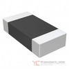
Single-layer PCBs are the simplest form and consist of a single conductive copper layer on one side of the board. These are cost-effective and often used in less complex devices that do not require advanced circuitry. For example, they are used in basic electronic toys, calculators, power adapters, and LED lighting systems. Not only does the copper layer conduct electricity but it is also protected by a solder mask to prevent oxidation. In addition, silkscreen printing on the PCB marks the location of components, simplifying assembly and maintenance.
Figure 4: Single-Layer PCB
In contrast, a double-layer PCB uses copper on both sides, allowing for more complex routing and circuit designs. This type is suitable for devices that require denser circuit configurations, such as mobile phones and power converters. The double-sided nature of these PCBs provides greater flexibility in designing circuits within limited space.

Figure 5: Double-Layer PCB
Multilayer PCBs add further complexity by containing three or more copper layers bonded with heat-resistant insulating glue. This structure not only enhances the mechanical strength of the circuit board but also can accommodate higher component density and more complex wiring configurations. Multilayer PCBs are important for high-performance devices such as computer motherboards, servers, medical imaging systems, and military electronics, where enhanced performance and reduced signal interference are important.
Figure 6: Multi-Layer PCB
In terms of materials, rigid PCBs dominate standard electronics due to their robustness and durability. However, the flexibility of flexible PCBs makes them ideal for modern applications where space is limited or where curved surfaces are involved, such as wearable technology and foldable smartphones.

Figure 7: Rigid PCB
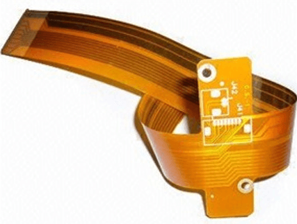
Figure 8: Flexible PCB
Rigid-flex PCBs combine the advantages of rigid and flexible PCBs, providing a hybrid solution that is structurally stable but flexible when necessary. This type is particularly useful in complex electronic devices that require complex wiring and flexible interconnections.
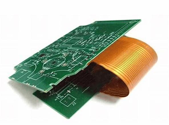
Figure 9: Rigid-Flex PCB
For applications that require minimal signal loss and interference, such as high-speed communications and radar equipment, high-frequency PCBs use materials such as Rogers or PTFE to optimize performance. In addition, aluminum-based PCBs are favored in high-power applications such as LED lighting and power amplifiers, where efficient heat dissipation is important.
Each PCB type is precision-engineered to ensure it meets the specific needs of its application, reflecting the innovation and versatility of PCB technology and its significant impact on modern electronic design.

Figure 10: Aluminum-Based PCB
How to Choose the Right PCB
Choosing the right printed circuit board (PCB) can help optimize the performance, reliability, and cost-efficiency of your electronic equipment. Below is a detailed guide to making an informed choice based on various operating and design requirements.
Circuit Complexity and Signaling Requirements: For simple or low-speed devices such as household appliances, a single- or double-sided PCB is usually sufficient. These PCBs are cost-effective and meet basic electrical connection needs. Conversely, for devices that operate at high speeds or frequencies, such as complex communications equipment or complex computer systems, multilayer PCBs are preferable. Multilayer PCBs provide greater routing space, better signal integrity, and reduced electromagnetic interference, which is beneficial in maintaining the functionality of complex circuits.
Material selection: Material selection depends largely on the operating frequency of the circuit and the operating temperature of the device. For high-frequency applications requiring minimal signal loss, materials such as Rogers or PTFE are ideal due to their low dielectric constant and loss rate. For equipment operating in high-temperature environments, choosing PCB materials that can withstand high temperatures can effectively prevent circuit failures.
Physical Space Considerations: The size and shape of the PCB must fit exactly into the device enclosure. This ensures that all components are installed correctly and that circuit failures do not occur due to physical limitations. For devices that need to be mounted on curved surfaces or require flexible wiring, options such as flexible PCBs or rigid-flex PCBs are available. They can be bent or folded to fit without compromising circuit integrity.
Thermal Management: Effective heat dissipation enables PCBs used in high-power applications or PCBs with densely packed components. PCBs made of materials such as aluminum or copper can effectively conduct heat away from critical components, preventing overheating and improving device reliability.
Cost considerations: While single-sided PCBs are typically the most economical, total lifecycle costs should also be considered, including maintenance, potential upgrades, and failure rates. It is important to design PCBs that adhere to standard manufacturing processes to minimize errors and additional costs.
Manufacturability and testability: The PCB design should be easy to manufacture and include test points for efficient troubleshooting. This not only helps maintain the quality during series production but also simplifies maintenance throughout the equipment's service life.
Environmental Compliance: It is important to select PCB materials and processes that comply with environmental standards such as RoHS (Restriction of Hazardous Substances). This ensures products are environmentally safe and compliant with market regulations, resulting in a smoother entry into the market.
By carefully evaluating aspects such as circuit needs, material properties, physical dimensions, thermal management, cost, manufacturability, and environmental compliance, you can select a PCB that perfectly meets your specific application requirements.
PCB Manufacturing Detailed Process
The process begins with the use of professional PCB design software such as Altium Designer, Eagle, or KiCad. Designers carefully lay out circuit diagrams, accurately position components, and develop power and ground connection strategies to ensure the design functions properly and meets manufacturing constraints. They also plan for future testing and assembly needs, aiming to minimize the likelihood and cost of subsequent changes.
Prototype testing tests the feasibility of the design. With rapid prototyping services, designers can identify and correct errors before they enter mass production, saving time and costs.
The pattern transfer stage involves transferring the circuit pattern onto the PCB substrate. This usually involves creating a mask and employing photolithography, or using direct methods such as laser or inkjet printing. The unwanted copper is then chemically etched away, leaving the intended conductive path.
Drill holes to create the necessary holes for the pin components and make electrical connections through vias. The precision here allows the holes to be aligned exactly with the design. The holes are then plated to enhance conductivity and connect the different PCB layers.
At this stage, solder mask ink is applied to areas not suitable for soldering. This layer prevents accidental solder connections during the soldering phase. Later, silk screens are added to mark component locations and other important data to aid assembly and future maintenance.
The final physical step is to cut the larger circuit board into individual PCBs and customize them to the specifications of the intended end product. Each PCB undergoes thorough inspection and electrical testing, such as flying probe testing, to detect any shorts, opens, or other defects, confirming that each board meets design and performance standards.
Precision, strict adherence to quality standards, and methodical progression at every stage contribute to PCB manufacturing, ensuring the reliability and functionality of the final product.
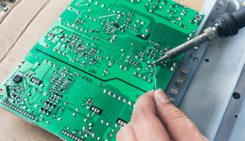
Figure 11: Manufacturing of PCB
What is PCBA?
Printed circuit board assembly (PCBA) is the process of mounting various electronic components, such as chips, resistors, and capacitors, onto a printed circuit board (PCB), transforming it into a functional electronic device. This critical step transforms a theoretical circuit design on a bare PCB into a practical working system. Once assembled, the PCBA becomes the operational core of the electronic product, facilitating key functions such as signal processing, power management, and user interface control. This stage brings the electronic design to life and enables the device to effectively perform its intended electronic function.

Figure 12: PCBA
Assembly Process of PCBA
The PCBA process begins with the procurement of key electronic components such as resistors, capacitors, integrated circuits (ICs), and connectors. Each component undergoes rigorous testing to verify compliance with design specifications and functional requirements. Ensuring the quality and performance of these components prevents problems later in production.
Component assembly is a fundamental part of the PCBA process. It mainly uses two methods: surface mount technology (SMT) and through-hole technology (THT). SMT is used to mount micro components on the PCB surface quickly and with high precision. This task is typically performed by automated placement machines, ensuring efficiency and accuracy. For components requiring additional mechanical strength, THT is preferred. Although THT may involve more physical labor, it provides the structural stability needed for certain parts of the PCB.
The soldering stage creates a strong connection between the component and the PCB. In SMT, reflow soldering is common, where solder paste is applied and then heated to form a strong solder joint. For THT components, wave soldering is used to achieve a strong and durable connection. Both soldering techniques are carefully controlled in terms of temperature and duration to protect delicate electronic components from thermal damage.
After soldering, the PCB assembly goes through various tests to ensure accurate placement and functionality. This includes visual inspection, automated optical inspection (AOI), X-ray inspection, and electrical functional testing. These inspections help detect and correct any defects or errors in the assembly, ensuring the circuit operates as expected.
Once testing confirms that the assembly is free of defects, the PCBA is cleaned to remove any soldering residue that may affect performance. The components are then carefully packaged to prevent damage during shipping or storage, ensuring they are in optimal condition when the final product is assembled.
The entire PCBA process requires a high degree of technical skills and strict adherence to quality control protocols. PCBA ensures that electronic equipment is reliable and able to meet advanced technical requirements and market expectations through meticulous assembly technology and rigorous testing.

Figure 13: Assembly of PCBA
Key Design Factors to Optimize PCBA Manufacturability and Yield
During the initial design phase, it is critical to select components that are standard in size and easy to use. These standard components simplify the assembly process, reduce costs, and improve assembly efficiency. Larger parts are generally easier to handle and assemble than micro parts, whether manually or automatically. This consideration helps minimize assembly errors and production delays related to supply issues.
A carefully planned layout prevents component collisions and promotes efficient assembly. Adequate spacing of components allows for better heat dissipation and easier maintenance, thereby enhancing the overall durability and functionality of the PCBA.
Incorporating redundant paths into the circuit design enhances the reliability of the PCBA. This design strategy ensures that if a certain circuit section fails, the system can still continue to operate, thereby improving the product's operational reliability.
Effective thermal management helps maintain the long-term performance and stability of PCBAs. Designs that evenly distribute heat-generating components help avoid hot spots. Including radiators, heat pipes, or ensuring adequate air circulation can effectively dissipate heat.
Optimizing the size and layout of pads and vias can significantly improve soldering quality and connection reliability. Properly sized and spaced pads help prevent solder bridging, while carefully designed vias enhance the mechanical strength and electrical integrity of multi-layer connections.
Clearly marking the component location, polarity, and other critical information directly on the PCB helps reduce assembly errors and simplifies testing and maintenance. Designing multiple PCBs on a single panel (panelization) can also increase manufacturing efficiency and reduce costs.
Integrating a consistent test strategy during the design phase, including retaining appropriate test points, facilitates efficient circuit testing. This proactive approach helps identify and correct defects in a timely manner, ensuring consistency and reliability in batch production.
Using tools like Design Rule Checking (DRC) and Manufacturing Rule Checking (MRC) in PCB design software ensures that the design complies with manufacturing and testing standards. These tools help identify and resolve potential design issues early, avoiding costly delays and revisions during production.
By addressing these critical factors during the design stage, designers can significantly improve PCBA manufacturability and yield. This not only minimizes potential risks and costs but also ensures that the final product meets high quality and performance standards, maintaining production efficiency and cost-effectiveness.
What is the Difference Between PCB and PCBA?
A Printed Circuit Board (PCB) is a flat, rigid board that forms the foundation of electronic circuits. It consists of multiple layers such as a non-conductive base material, often fiberglass, topped with layers of conductive copper traces. These traces are the pathways that enable electrical connections between various electronic components. The PCB also includes features like pads and through-holes specifically designed to secure and connect these components. However, at this stage, the components are not yet added to the board.
On the other hand, a Printed Circuit Board Assembly (PCBA) is a PCB that has been fully assembled with all its electronic components. This includes the soldering of components like resistors, capacitors, and integrated circuits onto the PCB. The assembly process requires careful placement of components, precise soldering, and thorough testing to ensure the board functions correctly. PCBA transforms a bare PCB into a complete, operational module capable of performing electronic tasks.
In terms of functionality, a PCB alone is inactive; it does not function electronically as it lacks components. It serves primarily as the structural base that allows for the layout and connection of electronic components. A PCBA, however, is an active, fully functional entity. With all components installed and interconnected, the PCBA is ready to fulfill specific electronic functions in devices.

Figure 14: PCB Assembled into PCBA
Conclusion
The creation of PCBs (Printed Circuit Boards) and PCBAs (Printed Circuit Board Assemblies) is a complex process that requires careful consideration of various factors. These factors include electrical performance, mechanical configuration, the component's ability to handle heat (thermal management), the type of materials used, and the specific manufacturing technology applied. The PCB is essentially the backbone of any electronic device, providing the framework upon which all other components are mounted. It can be thought of as the skeleton of an electronic device. In contrast, a PCBA represents a complete structure that contains not just the skeleton but also the muscle—electronic components such as capacitors, resistors, and integrated circuits. These components enable the device to operate efficiently and bring static PCBs to life. The process of manufacturing electronic products starts with PCB, which lays the foundation. The completion of the PCBA marks the pinnacle of the production process, transforming the PCB from a mere carrier of potential into a functional electronic unit. Recognizing the differences between PCB and PCBA is important to fully understand the entire life cycle of an electronic product, from design to execution.
To ensure that these products meet the high standards required by today's market, established design and manufacturing protocols must be strictly adhered to. Additionally, continuous advancements in technology and a strong commitment to quality control play an important role in improving the reliability and performance of these electronic products.
Frequently Asked Questions [FAQ]
1. What is the difference between a PCB and a breadboard?
A key distinction lies in the construction and flexibility of these components. Breadboards are not designed for permanent setups as they do not require soldering, allowing for easy modification and removal of components. On the other hand, PCBs have components that are either surface-mounted or through-hole-mounted, making them more durable and suitable for long-term applications.
2. What makes up a PCB and PCBA?
PCBA stands for Printed Circuit Board Assembly, which includes all the necessary components already installed and ready for deployment. These components, which are integral to the functioning of the PCB, may include capacitors, inductors, resistors, diodes, transistors, modules, and BGAs.
3. How does circuit design differ from PCB design?
Once the schematic design, which is the top-level document, is completed, the electronic circuit design is considered complete. All other design documents stem from this schematic. PCB design specifically focuses on converting these schematics into the physical form of a printed circuit board.
4. How can one identify a PCB?
Most PCBs are marked with a two-part identification system on their surfaces. The first part helps in identifying the PCB when it is bare without any electronic components. The second part is used for identification once electronic components are soldered onto the surface or mounted through holes.
5. What is the most common type of PCB?
The single-sided PCB is the most prevalent type. It features a conductive copper layer on one side of the substrate. Electronic components are soldered or placed on this side, while the etched circuits are visible on the opposite side. This configuration simplifies the design and manufacturing processes, making it a popular choice for many basic electronics applications.
Related Blog
-
Fundamentals of Op-Amp Circuits
![Fundamentals of Op-Amp Circuits]()
December 28th, 2023
In the intricate world of electronics, a journey into its mysteries invariably leads us to a kaleidoscope of circuit components, both exquisite and co... -
How Many Zeros in a Million, Billion, Trillion?
![How Many Zeros in a Million, Billion, Trillion?]()
July 29th, 2024
Million represents 106, an easily graspable figure when compared to everyday items or annual salaries. Billion, equivalent to 109, starts to stretch t... -
Comprehensive Guide to SCR (Silicon Controlled Rectifier)
![Comprehensive Guide to SCR (Silicon Controlled Rectifier)]()
April 22th, 2024
Silicon Controlled Rectifiers (SCR), or thyristors, play a pivotal role in power electronics technology because of their performance and reliability. ... -
CR2032 lithium-ion battery: multi-scenario applications and its unique advantages
![CR2032 lithium-ion battery: multi-scenario applications and its unique advantages]()
January 25th, 2024
The CR2032 battery, a commonly used coin-shaped lithium-ion battery, is essential in many low-power electrical products such as digital watches and po... -
NPN and PNP Transistors
![NPN and PNP Transistors]()
December 28th, 2023
For exploring the world of modern electronic technology, understanding the basic principles and applications of transistors is essential. Although the... -
What is a thermistor
![What is a thermistor]()
December 28th, 2023
In the realm of modern electronic technology, delving into the nature and working mechanism of thermistors becomes a crucial endeavor. These precision... -
Explore the Difference Between PCB and PCBA
![Explore the Difference Between PCB and PCBA]()
April 16th, 2024
A PCB serves as the backbone of electronic devices. Made from a non-conductive material, it physically supports components while also connecting them ... -
BC547 Transistor Comprehensive Guide
![BC547 Transistor Comprehensive Guide]()
July 4th, 2024
The BC547 transistor is commonly used in a variety of electronic applications, ranging from basic signal amplifiers to complex oscillator circuits and... -
What Is A Solenoid Switch
![What Is A Solenoid Switch]()
December 26th, 2023
When an electrical current flows through the coil, the resulting magnetic field either attracts or repels the iron core, causing it to move and either... -
IRLZ44N MOSFET Datasheet, Circuit, Equivalent, Pinout
![IRLZ44N MOSFET Datasheet, Circuit, Equivalent, Pinout]()
August 28th, 2024
The IRLZ44N is a widely-used N-Channel Power MOSFET. Renowned for its excellent switching capabilities, it is highly suited for numerous applications,...


Hot Parts
- 06035A6R2CAT2A
- CY7C1041DV33-10ZSXIT
- UC3875QF
- EP1AGX50DF780C6N
- CL03B221KO3NNND
- CC0201JRNPO8BN330
- MAX3238IDB
- ADDI7018XCPZ
- AD822AN
- CL31C101JJHNNNF
- IR2136JPBF
- A42MX36-PQ208I
- SI4435BDY-T1-GE3
- 1812HA390JAT1A
- GRM188R72D222KW07D
- PIC16F72-I/SO
- MCC162-12IO8
- TPSB107K006R0400
- L78M05CDT
- AD9958BCPZ
- P189A2002
- PMB2420SV2.3G
- ADS7955SDBT
- AD7192BRUZ
- SC900505BF
- IS42S32200B-6T
- AT45DB081E-SSHN-T
- X02047-012B-G0
- 0201ZA470JAT2A
- BS62LV2009STC-55
- MD7IC2755NR1
- LTC2970IUFD#TRPBF
- SKM145GAL174DN
- C1608X5R1V335K080AC
- STM1831L24WY6F
- MMBFU310LT1G
- VI-26L-CV
- T491C226M020ZTAU00
- F971C476MNCHT3
- LMZ31710RVQR
- AD9954YSV
- PMI156RC
- SD6106NFI
- SUM2035GAS2
- Q1900C-1S3
- R7S721001VCBG
- MAR229FPST
- BD82QS67