- English
-
EnglishDeutschItaliaFrançais한국의русскийSvenskaNederlandespañolPortuguêspolskiSuomiGaeilgeSlovenskáSlovenijaČeštinaMelayuMagyarországHrvatskaDanskromânescIndonesiaΕλλάδαБългарски езикGalegolietuviųMaoriRepublika e ShqipërisëالعربيةአማርኛAzərbaycanEesti VabariikEuskeraБеларусьLëtzebuergeschAyitiAfrikaansBosnaíslenskaCambodiaမြန်မာМонголулсМакедонскиmalaɡasʲພາສາລາວKurdîსაქართველოIsiXhosaفارسیisiZuluPilipinoසිංහලTürk diliTiếng ViệtहिंदीТоҷикӣاردوภาษาไทยO'zbekKongeriketবাংলা ভাষারChicheŵaSamoa日本語SesothoCрпскиKiswahiliУкраїнаनेपालीעִבְרִיתپښتوКыргыз тилиҚазақшаCatalàCorsaLatviešuHausaગુજરાતીಕನ್ನಡkannaḍaमराठी
The Evolution of Integrated Circuits: From Transistors to Advanced Digital Systems
Catalog
In-Depth Analysis of Integrated Circuits (ICs)
Integrated circuits, commonly referred to as chips or microchips, are pivotal components of modern electronics. These consist of a semiconductor wafer where myriad microscopic resistors, capacitors, and transistors reside. The foundation of IC design is built on silicon processing technology, which allows these intricate circuits to be seamlessly integrated into a single, cohesive silicon unit. In practice, ICs have revolutionized the fields of computing, telecommunications, and consumer electronics by dramatically miniaturizing electronic systems and enhancing their performance and efficiency.
Over the decades, significant strides have been made in the miniaturization and capability enhancement of integrated circuits. The industry has embraced scaling techniques, leading to the development of processes such as photolithography and advanced fabrication methods like FinFETs. These advancements contribute to the ongoing increase in transistor density on chips, closely following Moore's Law. An often-underestimated aspect of these innovations is how they allow for more compact and efficient energy usage, directly impacting the operational efficiency of electronic devices, from smartphones to supercomputers.
Importance of Integrated Circuit Design

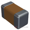
Figure 1: Integrated Circuit Chip
Core Objectives of IC Design
Integrated Circuit (IC) design focuses on forming connected circuit components that execute designated tasks. The core elements in this design include transistors, resistors, and capacitors. These components serve as the foundational units for crafting intricate functions, such as digital logic gates and analog amplifiers, which are critical in the functionality of sophisticated electronics like computers. By employing a full-custom design methodology, these elements can be meticulously engineered to satisfy precise design specifications.
Transition from Basic Components to Complex Systems
Transistors act as the switches within an electronic circuit, essential for processing digital signals. Resistors and capacitors regulate the flow of electricity and store energy, respectively. Through innovative arrangements and combinations, these basic components escalate into complex systems, catering to ever-evolving technological demands. Industry practices have shown that embracing cutting-edge software tools in the design phase significantly enhances efficiency and precision.
Real-World Application and Integration
IC designs are indispensable in various applications. From powering handheld devices to enabling smart appliances, their role continues to expand. The development of smaller and more powerful integrated circuits contributes vastly to the compactness and potency of modern gadgets. For instance, by learning from prior experiences, engineers have developed ICs with increased speed and reduced energy consumption, showcasing the importance of adapting designs to meet environmental and user needs.
Full-Custom Design Approach
The full-custom design approach in IC design emphasizes tailoring each element to achieve set objectives, epitomizing precision and innovation. This method allows for maximum optimization, providing bespoke solutions to complex challenges. Drawing from experience, engineers adept at this approach often anticipate and resolve potential challenges in the design stage, thereby enhancing the overall reliability and performance of the final product.
Varieties of Integrated Circuit Chips
Integrated Circuit (IC) chips are pivotal to modern electronics, existing in multiple forms that cater to diverse applications. The three principal types are Digital, Analog, and Mixed Integrated Circuits, each serving distinct roles in technology advancement.
Digital Integrated Circuits
Digital ICs are the backbone of modern computing and communication. They process discrete values, primarily ones and zeros, embodying the essence of binary computation. Examples include microprocessors, memory chips, and logic gates, central to devices like computers and smartphones. The constant pursuit of miniaturization and power efficiency in these components has significantly influenced the evolution of electronic devices over time. This ongoing trend not only furthers Moore's Law but also drives innovations in various sectors, including artificial intelligence and machine learning, which relentlessly seek more computing power and energy-saving solutions.
Analog Integrated Circuits
Analog ICs manage continuously variable signals. These circuits amplify, filter, and modify real-world analog signals such as sound, temperature, and light. Common applications include audio amplifiers and radio frequency communication systems. The design complexities of Analog ICs typically demand more expertise than their digital counterparts, as they must cater to a broader range of variabilities and conditions. Expertise in handling these intricacies often culminates in high-fidelity performance in consumer electronics, enabling more immersive experiences — whether it be through crisp audio in music systems or clearer signals in telecommunication.
Mixed-Signal Integrated Circuits
Mixed ICs, uniting both digital and analog functions, represent an integration milestone in circuit design. These versatile components are the foundation of many modern devices, including smartphones, smart meters, and automotive systems. As technology needs evolve, mixed ICs are imperative for seamless interfacing between the digital and analog realms. Designers face the challenge of optimizing these circuits for both functionality and efficiency, reflecting the industry's emphasis on developing cohesive, adaptable solutions for increasingly interconnected environments.
Exploring the Fundamentals and Applications of Digital Integrated Circuits
Digital Integrated Circuits are an essential component in modern electronics, executing tasks primarily through the manipulation of digital signals. They operate using binary codes, represented by 0 and 1, performing complex functions by employing logic gates such as AND, OR, and NOT. These logic gates form the foundation of digital systems, enabling them to process data with precision and efficiency.

Figure 2: Different Digital IC Devices
Classification and Characteristics of Digital ICs
Digital ICs are broadly categorized into Bipolar and Metal-Oxide-Semiconductor (MOS) families. The Bipolar family typically offers faster switching speeds but at the cost of higher power consumption. In contrast, MOS circuits are valued for their lower power requirements and high density, making them suitable for extensive integration. This classification is significant as it guides the selection of components based on specific application requirements, balancing performance and efficiency.
Bipolar Family of Digital ICs
Within the Bipolar category, transistors operate using both electron and hole charge carriers, facilitating rapid transitions ideal for high-frequency applications. This preference is often observed in situations demanding speed, such as in RF amplifiers and high-performance processors. Practitioners in the field often weigh the trade-offs between speed advantages and power conservation when deciding on circuit designs.
MOS Family of Digital ICs
MOS technology, characterized by metal-oxide-semiconductor field-effect transistors (MOSFETs), dominates digital integrated circuits thanks to its scalability and energy efficiency. Suitable for memory chips and microcontrollers, the widespread implementation of MOS ICs reflects an industry trend toward miniaturization and growing computational needs without proportionately increased power requirements.
Role in Instrumentation, Communications, and Computing
Digital Integrated Circuits play pivotal roles across various sectors, notably in instrumentation, communications, and computing. The ability to execute complex operations reliably makes them indispensable in microprocessors and digital signal processors. In the realm of telecommunications, they form the backbone of modern data transmission, enabling everything from basic telephony to expansive internet services. Additionally, these circuits are critical in numerous computing applications, forming the core of microarchitecture designs in computers.
Digital IC Design Process
Introduction to Digital IC Design
Designing digital integrated circuits (ICs) is a sophisticated process that involves crafting circuits to execute logical functions by converting digital inputs into binary codes. This intricate task requires the integration of numerous electronic devices through conductive pathways, with the objectives of innovating new electronic solutions or enhancing current technologies.
Key Stages in Digital IC Design
Specification and Design Requirements
At the outset, defining the specific requirements and performance standards is crucial. This entails a thorough understanding of the desired functionality, power consumption, and operating environments. Experienced engineers often recall that clear design specifications can prevent costly redesigns in later stages.
System Architecture Development
Developing a robust system architecture forms the backbone of the IC design process. It involves establishing a blueprint that ensures each component synergizes to fulfill the project’s goals. Discussions often arise around the trade-offs between performance and area efficiency, highlighting the importance of informed decision-making.
Logic Design and Verification
Logic design requires converting high-level specifications into detailed logic gate circuits. Verification is equally vital, employing simulation tools to ensure logical correctness. Even seasoned developers underscore the necessity of iterative testing, recognizing that early detection of errors can significantly curtail development timelines.
Physical Design and Layout
Transforming the logical design into a physical layout demands meticulous attention to detail. This step involves placing and routing the circuits within the confines of a silicon chip. Practical experience teaches that anticipating potential layout complications during early design phases can alleviate manufacturing challenges significantly.
Fabrication and Testing
Once the design is finalized, the fabrication process begins, transforming the virtual designs into tangible chips. Rigorous testing follows, encompassing functional, electrical, and environmental evaluations to verify performance. Anecdotal insights emphasize the criticality of comprehensive testing in ensuring reliability and mitigating post-production issues.
Challenges and Considerations
Technological Complexity
As technology progresses, the complexity of IC design escalates. Design professionals often remark that staying abreast of technological advancements and maintaining a flexible learning approach are key strategies for coping with this complexity.
Cost and Resource Management
Balancing budgetary constraints with the demands of high-quality IC design remains a persistent concern. Prioritizing resource optimization and leveraging cutting-edge design technologies can offer a path forward in maintaining cost-effectiveness while achieving excellence.
Digital IC Series
Digital IC series form the backbone of modern electronic circuits, playing a crucial role in both consumer electronics and industrial applications. Among the most influential are the 7400 and 4000 series, known for their versatility and reliability.
Overview of Key Digital IC Series
The 7400 series, developed by Texas Instruments, is formatted using TTL (Transistor-Transistor Logic) technology. It includes models like the 7402, a quad 2-input NOR gate, that are integral to constructing logical operations and arithmetic functions in electronic devices. The widespread adoption of these components is attributed to their robust performance across varying environmental conditions, an advantage for designers facing diverse operational contexts.
Success and Influence of the 4000 Series
Meanwhile, the 4000 series, based on CMOS (Complementary Metal-Oxide-Semiconductor) technology, offers benefits in terms of power consumption. For instance, the 4071 model, a quad 2-input OR gate, is favored for applications that require low power usage without compromising high noise immunity. The design philosophies underpinning these ICs emphasize efficiency, a guiding principle for engineers striving to balance cost and functionality in their designs.
Digital IC Logic Families
Overview of Digital IC Logic Families
Digital Integrated Circuit (IC) logic families are a foundational component in the design and functionality of electronic systems. These families, such as Diode Logic (DL), Resistor-Transistor Logic (RTL), and Transistor-Transistor Logic (TTL), among others, offer diverse options depending on application needs. Each logic family possesses unique characteristics such as speed, power consumption, and complexity, which are crucial in determining their suitability for various technological applications.
Diode Logic (DL)
Characteristics and Applications
Diode Logic uses diodes to perform logical operations, primarily basic AND and OR operations. Although simple and cost-effective, it is limited by a lack of amplification, leading to incomplete signal restoration. Modern technology rarely employs DL due to these constraints. Industry insights from early electronics highlight its significance during the nascent stages of digital design when simplicity and cost were critical factors.
Resistor-Transistor Logic (RTL)
Advantages and Limitations
Resistor-Transistor Logic, which utilizes resistors and transistors, represents a straightforward evolution from DL. RTL circuits offer faster operation and amplification capabilities, allowing signals to be restored to standard logic levels. Despite these improvements, RTL exhibits considerable power dissipation, especially at higher speeds, thus limiting its contemporary application. However, understanding its historical impact provides valuable lessons for modern eco-design approaches seeking minimalistic design with improved energy efficiency.
Transistor-Transistor Logic (TTL)
Impact and Evolution
Transistor-Transistor Logic overcomes many of the deficiencies found in previous families. TTL’s robustness, speed, and ability to drive multiple other circuits make it a staple in digital electronics. TTL's design pioneered higher integration levels in earlier microprocessors and still finds applications in education and basic electronics due to its reliability and ease of use. The advent of more sophisticated technologies owes much to TTL's foundational contribution to electronics design.
Comparative Analysis of Logic Families
Selection Considerations
When selecting a logic family, considerations include power efficiency, speed, cost, and complexity. Practical experience often dictates that applications with lower power requirements and higher speed demands may better leverage more advanced families like CMOS. However, each project's unique requirements can make even older logic families like TTL preferred for simplicity and educational purposes. Additionally, understanding the operational principles and constraints of each logic family can enhance innovative electronics design and development.
Comprehensive Steps in Digital IC Design
Digital IC design is a complex process entailing several critical stages, each crucial for the successful development of an integrated circuit. The process typically unfolds through a systematic series of steps: System Definition, Architectural Design, Logic and Circuit Design, Physical Design, Verification, Mask Preparation, Fabrication, and Testing. Each step contributes uniquely to the integrity and efficiency of the final product.

Figure 3: Design Flow of Digital IC
System Definition
The foundation of digital IC design starts at the system definition stage. This phase involves specifying the system's overall objectives, functional requirements, and performance benchmarks. A clear understanding of these parameters sets the stage for a design that meets specific user needs and constraints. Practical experience shows that investing time in precise system definition can significantly reduce the risk of design errors and project delays later on.
Architectural Design
Once the system is defined, the next challenge is to develop a robust architectural design. Here, designers delineate the high-level structure, identifying key modules and their interconnections. It is an iterative process, often requiring revisiting initial design assumptions. The insights gained from prior projects highlight that a flexible design, allowing for future modifications, is beneficial in managing unforeseen changes.
Logic and Circuit Design
At this stage, the focus shifts to logic and circuit design, where schematic diagrams and logical gates come to life. Designers transform architectural designs into realizable circuits, carefully considering optimization for speed, power, and area. It has been found that frequent design reviews and simulations help in anticipating and resolving potential issues.
Physical Design
Physical design involves translating logical circuits into physical layouts that can be fabricated on silicon. This step requires intricate knowledge of layout techniques and design rules. The lessons from industry practice indicate that collaboration between layout designers and circuit designers is essential to ensure that the physical design remains true to the intended logical design.
Verification
Verification ensures that all parts of the IC function correctly and meet the design specifications. Through rigorous testing, any discrepancies between the intended and actual design can be identified and rectified. The comprehensive verification process, often involving multiple methods and tools, underscores its role as a safeguard against costly design errors.
Mask Preparation
Once verification is complete, mask preparation is undertaken. This step translates the verified design into a set of masks, which serve as templates for the subsequent fabrication process. A nuanced understanding of fabrication techniques and processes allows designers to anticipate potential issues at this stage.
Fabrication
In the fabrication phase, the physical IC is manufactured based on the masks created. This intricate process involves numerous steps, including doping, etching, and layering, requiring meticulous precision. Insights from long-term project observations emphasize that close communication with the fabrication team can mitigate risks associated with manufacturing defects.
Testing
Finally, the testing phase validates the functionality and performance of the fabricated ICs under real-world conditions. Comprehensive testing can identify faults that may not have been evident in earlier design stages. Experienced engineers recognize the importance of testing as an opportunity to gather data that can inform future design improvements.
Key Aspects of Digital IC Design
Propagation Delay
Propagation delay denotes the time interval required for a logic gate to produce a stable output after accepting an input signal. Reducing this delay is instrumental in augmenting the overall system performance and achieving more responsive circuits. Remarkably, this delay often challenges designers as they strive to balance speed and circuit complexity.

Figure 4: Propagation Delay of Digital Logic

Figure 5: Propagation delay of Logic Hate
Fan-In
Fan-in represents the number of inputs a logic gate can efficiently process. An increased fan-in complicates gate design and may introduce potential performance setbacks, influencing not only the logical architecture but also the fabrication process.

Figure 6: Comparison Between Fan-In and Fan-Out
Fan-Out
Fan-out helps determine how many gates a single output can effectively drive, which plays a vital role in circuit functionality and integrity. A balanced fan-out preserves signal strength across the architecture and aids in minimizing load-induced delays.

Figure 7: Fan-Out Diagram
Noise Margin
Noise margin is a critical quantifier of a gate's ability to resist noise, ensuring systemic robustness by defining the voltage variation permissible without affecting signal stability. It acts as a safeguard, allowing designers to anticipate and mitigate potential interference.
Power Dissipation
Every functioning digital IC encounters power dissipation—both static and dynamic. Static dissipation arises when the circuit is idle, while dynamic dissipation occurs amid state transitions. Optimizing these aspects is essential for efficient power management, highly desirable in portable electronics.
Static and Dynamic Power Supply Needs
Digital ICs demand precise power levels, which are facilitated through supply voltages such as VCC or VDD. This requirement is pivotal for sustaining optimal operation and maximizing device longevity. Thorough planning in this area is recognized for enhancing both durability and performance.
Temperature and Reliability Metrics
Operating across a spectrum of temperatures, digital ICs—especially military-grade—are engineered to withstand extreme conditions. Performance speed, reliability, and power consumption emerge as key evaluation metrics. Designers undertake comprehensive testing to maintain functionality under adverse conditions.
Pros and Cons of Digital ICs
Digital ICs provide substantial benefits, including low power consumption and enhanced reliability. Nonetheless, challenges exist, such as noise handling limitations and power ratings that demand strategic problem-solving in design approaches.
Applications of Digital ICs
Digital ICs are foundational to myriad technologies, empowering computers, logic devices, memory modules, and amplifiers. Their adaptability and indispensability are evident in the evolution of modern electronics, underlining their pivotal role and enduring impact on technological progress.
Related Blog
-
Fundamentals of Op-Amp Circuits
![Fundamentals of Op-Amp Circuits]()
December 28th, 2023
In the intricate world of electronics, a journey into its mysteries invariably leads us to a kaleidoscope of circuit components, both exquisite and co... -
How Many Zeros in a Million, Billion, Trillion?
![How Many Zeros in a Million, Billion, Trillion?]()
July 29th, 2024
Million represents 106, an easily graspable figure when compared to everyday items or annual salaries. Billion, equivalent to 109, starts to stretch t... -
Comprehensive Guide to SCR (Silicon Controlled Rectifier)
![Comprehensive Guide to SCR (Silicon Controlled Rectifier)]()
April 22th, 2024
Silicon Controlled Rectifiers (SCR), or thyristors, play a pivotal role in power electronics technology because of their performance and reliability. ... -
CR2032 lithium-ion battery: multi-scenario applications and its unique advantages
![CR2032 lithium-ion battery: multi-scenario applications and its unique advantages]()
January 25th, 2024
The CR2032 battery, a commonly used coin-shaped lithium-ion battery, is essential in many low-power electrical products such as digital watches and po... -
NPN and PNP Transistors
![NPN and PNP Transistors]()
December 28th, 2023
For exploring the world of modern electronic technology, understanding the basic principles and applications of transistors is essential. Although the... -
What is a thermistor
![What is a thermistor]()
December 28th, 2023
In the realm of modern electronic technology, delving into the nature and working mechanism of thermistors becomes a crucial endeavor. These precision... -
Explore the Difference Between PCB and PCBA
![Explore the Difference Between PCB and PCBA]()
April 16th, 2024
A PCB serves as the backbone of electronic devices. Made from a non-conductive material, it physically supports components while also connecting them ... -
BC547 Transistor Comprehensive Guide
![BC547 Transistor Comprehensive Guide]()
July 4th, 2024
The BC547 transistor is commonly used in a variety of electronic applications, ranging from basic signal amplifiers to complex oscillator circuits and... -
What Is A Solenoid Switch
![What Is A Solenoid Switch]()
December 26th, 2023
When an electrical current flows through the coil, the resulting magnetic field either attracts or repels the iron core, causing it to move and either... -
IRLZ44N MOSFET Datasheet, Circuit, Equivalent, Pinout
![IRLZ44N MOSFET Datasheet, Circuit, Equivalent, Pinout]()
August 28th, 2024
The IRLZ44N is a widely-used N-Channel Power MOSFET. Renowned for its excellent switching capabilities, it is highly suited for numerous applications,...


Hot Parts
- SCC68692C1N40,602
- ICL8048BCJE
- SRM2A256SLM70A
- R5F10RFCAFP#V0
- XL4015E1
- LC75813TS-E
- UC2845N
- SAA1043T
- AD9806KSTZRL
- TAJB105M035H
- M63032FP
- R5F104GCAFB#V0
- F3L300R12ME4_B23
- LCMXO2-2000HC-4TG144I
- FM218SM1
- PCF8564ACX9/1
- TMS32C6203BGNZA250
- HC7356-37R-LF1
- M74HC74M1R
- LDK120DM33R
- MC74LCX14DTR2
- T491C226M016AS
- CC1812KKX7RBBB473
- VI-910705
- 06033A471F4T2A
- ACD2206S8P1
- GRM155R71C104KA88J
- MCC55-15IO2
- 1812HC152MAT1A
- 08051A3R0CAT4A
- E52HA2.2C-B
- MK2715-01S
- X9279TV14T1
- HY5DU283222BFP-33-C
- 12102C103KAT2M
- ADR02BUJZ-REEL7
- CY62256NLL-55SNXI
- LP2986AIMMX-5.0
- GMS3974RAA05F
- 12102U8R2BAT2A
- BYW54
- 9LPR501SGLFT
- HSR412-SR2M
- HA2-2522-8
- M29W320EB70ZE
- LTC7000JMSE#TRPBF
- 88E1512PB2-NNP2C000
- UPD750006GB-532-3B4